- 您现在的位置:买卖IC网 > Sheet目录3871 > PIC18F83J11T-I/PT (Microchip Technology)IC PIC MCU FLASH 4KX16 80TQFP
PIC18F85J11 FAMILY
DS39774D-page 166
2010 Microchip Technology Inc.
15.1
Timer3 Operation
Timer3 can operate in one of three modes:
Timer
Synchronous Counter
Asynchronous Counter
The operating mode is determined by the clock select
bit, TMR3CS (T3CON<1>). When TMR3CS is cleared
(= 0), Timer3 increments on every internal instruction
cycle (FOSC/4). When the bit is set, Timer3 increments
on every rising edge of the Timer1 external clock input
or the Timer1 oscillator, if enabled.
As
with
Timer1,
the
RC1/T1OSI
and
RC0/T1OSO/T13CKI pins become inputs when the
Timer1 oscillator is enabled. This means the values of
TRISC<1:0> are ignored and the pins are read as ‘0’.
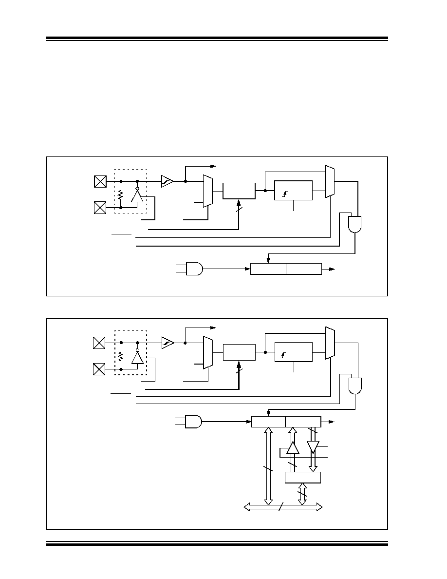
FIGURE 15-1:
TIMER3 BLOCK DIAGRAM (8-BIT MODE)
FIGURE 15-2:
TIMER3 BLOCK DIAGRAM (16-BIT READ/WRITE MODE)
T3SYNC
TMR3CS
T3CKPS<1:0>
Sleep Input
T1OSCEN(1)
FOSC/4
Internal
Clock
Prescaler
1, 2, 4, 8
Synchronize
Detect
1
0
2
T1OSO/T13CKI
T1OSI
1
0
TMR3ON
TMR3L
Set
TMR3IF
on Overflow
TMR3
High Byte
Timer1 Oscillator
Note 1: When enable bit, T1OSCEN, is cleared, the inverter and feedback resistor are turned off to eliminate power drain.
On/Off
Timer3
CCPx Special Event Trigger
CCPx Select from T3CON<6,3>
Clear TMR3
Timer1 Clock Input
T3SYNC
TMR3CS
T3CKPS<1:0>
Sleep Input
T1OSCEN(1)
FOSC/4
Internal
Clock
Prescaler
1, 2, 4, 8
Synchronize
Detect
1
0
2
T1OSO/T13CKI
T1OSI
Note 1: When enable bit, T1OSCEN, is cleared, the inverter and feedback resistor are turned off to eliminate power drain.
1
0
TMR3L
Internal Data Bus
8
Set
TMR3IF
on Overflow
TMR3
TMR3H
High Byte
8
Read TMR3L
Write TMR3L
8
TMR3ON
CCPx Special Event Trigger
Timer1 Oscillator
On/Off
Timer3
Timer1 Clock Input
CCPx Select from T3CON<6,3>
Clear TMR3
发布紧急采购,3分钟左右您将得到回复。
相关PDF资料
PIC16LF627-04/P
IC MCU FLASH 1KX14 COMP 18DIP
PIC18F86J55T-I/PT
IC PIC MCU FLASH 48KX16 80TQFP
PIC18F43K22-I/MV
MCU PIC 8KB FLASH 40QFN
PIC16C55A-04I/P
IC MCU OTP 512X12 28DIP
PIC18LF43K22-I/MV
MCU PIC 8KB FLASH 40UQFN
PIC16C622A-20I/P
IC MCU OTP 2KX14 COMP 18DIP
PIC18F84J11T-I/PT
IC PIC MCU FLASH 8KX16 80TQFP
PIC18F24K22-I/SP
IC PIC MCU 16KB FLASH 28SPDIP
相关代理商/技术参数
PIC18F83J90-I/PT
功能描述:8位微控制器 -MCU 8KB FL 1024b RAM 67I/O 8b Fam RoHS:否 制造商:Silicon Labs 核心:8051 处理器系列:C8051F39x 数据总线宽度:8 bit 最大时钟频率:50 MHz 程序存储器大小:16 KB 数据 RAM 大小:1 KB 片上 ADC:Yes 工作电源电压:1.8 V to 3.6 V 工作温度范围:- 40 C to + 105 C 封装 / 箱体:QFN-20 安装风格:SMD/SMT
PIC18F83J90T-I/PT
功能描述:8位微控制器 -MCU 8KB Flash 1024bytes-RAM 67I/O RoHS:否 制造商:Silicon Labs 核心:8051 处理器系列:C8051F39x 数据总线宽度:8 bit 最大时钟频率:50 MHz 程序存储器大小:16 KB 数据 RAM 大小:1 KB 片上 ADC:Yes 工作电源电压:1.8 V to 3.6 V 工作温度范围:- 40 C to + 105 C 封装 / 箱体:QFN-20 安装风格:SMD/SMT
PIC18F8410-E/PT
功能描述:8位微控制器 -MCU 16kBF 768RM 70I/O RoHS:否 制造商:Silicon Labs 核心:8051 处理器系列:C8051F39x 数据总线宽度:8 bit 最大时钟频率:50 MHz 程序存储器大小:16 KB 数据 RAM 大小:1 KB 片上 ADC:Yes 工作电源电压:1.8 V to 3.6 V 工作温度范围:- 40 C to + 105 C 封装 / 箱体:QFN-20 安装风格:SMD/SMT
PIC18F8410-I/PT
功能描述:8位微控制器 -MCU 16kBF 768RM 70I/O RoHS:否 制造商:Silicon Labs 核心:8051 处理器系列:C8051F39x 数据总线宽度:8 bit 最大时钟频率:50 MHz 程序存储器大小:16 KB 数据 RAM 大小:1 KB 片上 ADC:Yes 工作电源电压:1.8 V to 3.6 V 工作温度范围:- 40 C to + 105 C 封装 / 箱体:QFN-20 安装风格:SMD/SMT
PIC18F8410T-I/PT
功能描述:8位微控制器 -MCU 16kBF 768RM 70I/O RoHS:否 制造商:Silicon Labs 核心:8051 处理器系列:C8051F39x 数据总线宽度:8 bit 最大时钟频率:50 MHz 程序存储器大小:16 KB 数据 RAM 大小:1 KB 片上 ADC:Yes 工作电源电压:1.8 V to 3.6 V 工作温度范围:- 40 C to + 105 C 封装 / 箱体:QFN-20 安装风格:SMD/SMT
PIC18F8490-E/PT
功能描述:8位微控制器 -MCU 16kBF 768RM 66I/O RoHS:否 制造商:Silicon Labs 核心:8051 处理器系列:C8051F39x 数据总线宽度:8 bit 最大时钟频率:50 MHz 程序存储器大小:16 KB 数据 RAM 大小:1 KB 片上 ADC:Yes 工作电源电压:1.8 V to 3.6 V 工作温度范围:- 40 C to + 105 C 封装 / 箱体:QFN-20 安装风格:SMD/SMT
PIC18F8490-I/PT
功能描述:8位微控制器 -MCU 16kBF 768RM 66I/O RoHS:否 制造商:Silicon Labs 核心:8051 处理器系列:C8051F39x 数据总线宽度:8 bit 最大时钟频率:50 MHz 程序存储器大小:16 KB 数据 RAM 大小:1 KB 片上 ADC:Yes 工作电源电压:1.8 V to 3.6 V 工作温度范围:- 40 C to + 105 C 封装 / 箱体:QFN-20 安装风格:SMD/SMT
PIC18F8490-I/PT
制造商:Microchip Technology Inc 功能描述:IC 8BIT FLASH MCU 18F8490 TQFP80